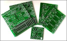
PCB fabrication, or Printed Circuit Board fabrication, is the process of manufacturing circuit boards used in electronic devices. It involves several steps to transform raw materials into functional PCBs. Let’s explore the details:
Definition and Purpose
Definition
PCB fabrication refers to the process of producing printed circuit boards, which are essential components in electronic devices for connecting and supporting electronic components.
Purpose
The purpose of PCB fabrication is to create high-quality circuit boards that meet the design specifications and performance requirements of electronic devices, ensuring reliability and functionality.
PCB Fabrication Process
Design Preparation
The fabrication process begins with the preparation of the PCB design files, including the layout of circuit traces, placement of components, and design specifications.
Substrate Material Selection
Selecting the substrate material is crucial, as it determines the PCB’s properties such as electrical conductivity, thermal conductivity, and mechanical strength. Common substrate materials include FR-4, aluminum, and flexible materials like polyimide.
Copper Cladding
The substrate material is clad with a thin layer of copper on both sides, forming the conductive layers of the PCB.
Imaging
The PCB design is transferred onto the copper-clad substrate using a photosensitive material or a stencil. This step defines the circuit pattern and traces on the PCB.
Etching
The exposed copper areas not protected by the imaging process are etched away using chemical solutions, leaving behind the desired circuit traces.
Drilling
Small holes, called vias, are drilled into the PCB to allow for component mounting and electrical connections between different layers of the board in multilayer PCBs.
Plating
Plating processes, such as electroplating or chemical deposition, are used to deposit additional layers of copper onto the PCB surfaces and inside the vias, enhancing conductivity and ensuring proper electrical connections.
Surface Finish
The PCB surfaces are coated with a surface finish material, such as solder mask or gold plating, to protect the copper traces, improve solderability, and enhance the PCB’s overall durability.
Testing and Inspection
After fabrication, the PCBs undergo rigorous testing and inspection processes to verify functionality, electrical continuity, and quality, ensuring compliance with design specifications and industry standards.
Benefits of PCB Fabrication
Customization
PCB fabrication allows for customization of circuit designs, sizes, and specifications to meet the unique requirements of electronic devices and applications.
Cost Efficiency
Mass production of PCBs through fabrication processes enables economies of scale, reducing per-unit costs and making PCBs more cost-effective for electronic manufacturers.
Quality Assurance
Fabricated PCBs undergo stringent quality control measures, ensuring consistency, reliability, and performance across production batches.
Scalability
PCB fabrication processes are scalable to accommodate varying production volumes, from prototype runs to high-volume manufacturing, providing flexibility and responsiveness to customer demand.
Innovation
Advancements in PCB fabrication technologies and materials drive innovation in electronic design and manufacturing, enabling the development of smaller, faster, and more efficient electronic devices.
PCB fabrication plays a critical role in the electronics industry, providing the foundation for the production of a wide range of electronic devices. Explore more about PCB fabrication at pcb fabrication.

